


Description:
ANDTech provides Custom Made Electronic Design, engaged in theR&D, specialized in the rapid prototyping, customizedelectronics.Our team can provide youwith the support services you need to get your projects done - andon schedule!
Whychoose ANDTech?
Our layout team can do a complete layout project or help withsmaller portions such as placement studies, routing, generatingproper manufacturing files, library management, and more. Weare happy to make small changes or complete large complexdesigns.
We understand that our customers often need a PCB designcompleted quickly. We support our customers by providingexpedited PCB layout service at no additional hourly cost.
We provide quotes on an hourly basis (time and materials) orwith a fixed price. Call us today to find out how we can improveyour design quality, meet your deadlines, and save money.
AND Technologies offers the fastestturnaround to reach the prototype stage, followed by quicktransition to production and volume manufacturing.
Ourengineer Team is professional and partner factory is highlyequipped with advanced manufacturing facilities and machines. wecan do for you at low cost but high quality.
- hardware design(circuit design , PCB layout).According tocustom-requirement
- software and firmware design, of MCU, DSP, embedded system ,ARM
- Mechanical design(2D, 3D drawing), tooling and moldingdesign
- integration and prototyping. finish a full-functionproducts
- mass production and upgrade of existing designs
we will protect the intellectual property of the product for ourcustomers.
Massproduction is the production of large amounts of standardizedproducts, including and especially on.
- High-Density BGAs, QFNs, Micro-Vias, Ultra-Fine Trace andSpace
- Hand-Crafted Layout for Memory Systems, Chipsets, High-SpeedDesigns
- Layout Planning for High-Current Applications (Power Supplies,Motor Control) Minimizing Current Loops
- RF Layout Strategies
- Design for EMI Compliance
- Design for Manufacturability Stack-Up, Spacing, IPCFootprints
- Specialty Design Considerations
- Controlled Impedance
- High-Speed PCB Materials
- Blind and Buried Vias Thermally Conductive PCB Materials
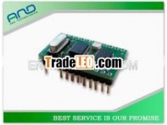
- Electronic design about motor driver, PCB Layout Design,Circuit Design, SMT, schematics design, Technical support
Thanks for your dropping by! Please let me know what you thinkof the electronic design!
For over 8 years PCB Assembly has been deliveringsuperior quality and on-time delivery to itscustomers.
We will handle your order with the greatest care andresponsibility. Give us a try, you will be happy youdid!
OurFactory Manufacture Capability
Item | Manufacture Capability |
Board Material | FR-4 |
Layer | 1-20 |
Finished Board thickness | 0.2 mm-3.8mm ( 8 mil-150 mil ) |
Board Thickness Tolerance | ±10% |
Copper thickness | 0.5 OZ--2.0OZ |
Impedance Control | YES |
Hole tolerance | PTH:±0.075mm NPTH: ±0.05mm |
Min drilled Hole size | 0.15mm(6mil) |
Min Laser hole size | 0.1mm(4mil) |
Min Space Width | 0.075mm (3 mil) |
Min Trace Width | 0.075mm(3mil) |
BGA Pitch | 0.2 mm (8 mil) |
Solder mask Color | Green , Red , Blue , Black , White |
Panel Outline Tol (/-) | CNC: ±0.125mm, Punching: ±0.15mm |
Surface finish/treatment | HASL/HASL lead free , Immersion Gold |
Certificate | ROHS, ISO9001:2008, SGS, UL certificate |
Custom-Made Electronic Design with electronical products
